Tin Whiskering
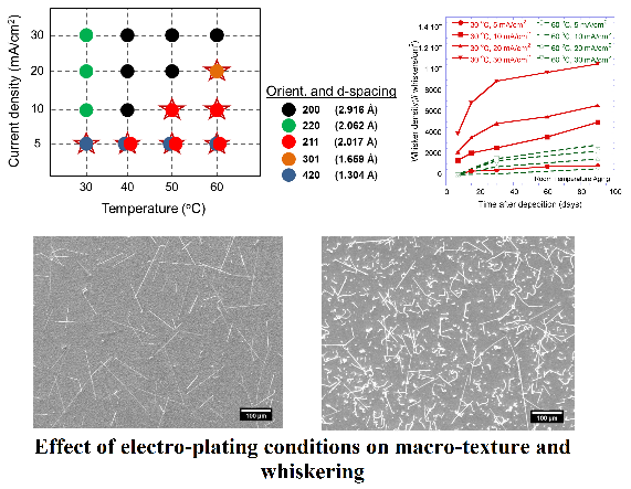
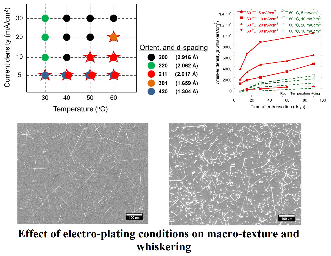
Currently, the effects of thermo-electro-environ-mechanical excursions on tin-whiskering are being studied. The effects of under-layers, over-layers and minority alloying elements on whisker propensity will also be studied. Piyush Jagtap is working on this problem.
We have found that the macro-texture of the Sn coats significantly affects whiskering in Sn films electroplated on brass substrate. Interestingly, electroplating conditions greatly influence the macro-texture. Hence, tailoring electroplating conditions (namely, bath temperature and current density) can help in controlling whisker growth.
Development of Thermal Interface Materials (TIMs) and Interconnects (ICs) for Next Generation Microelectronic Packaging
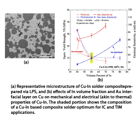
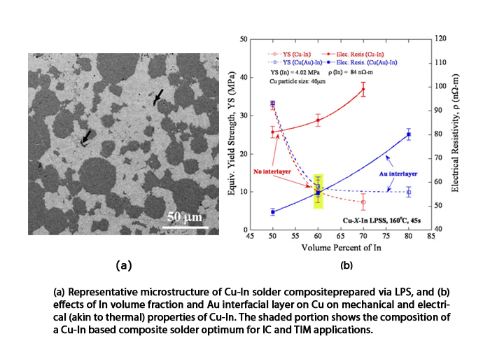
Thermal interface materials should have high thermal conductivity and high shear compliance. Such materials may be produced via liquid phase sintering (LPS), which enables uniform distribution of the high melting phase (HMP) constituents in the low melting phase (LMP) matrix. The thermal conductivity of optimized Cu-In based solders was shown to be at least 2 times higher than that of pure In with only ~50% increase in the yield strength of the composite relative to the pure indium.
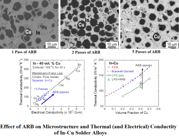
Currently, we are striving to improve the thermal and mechanical properties of Cu-In composites by adopting a two steps procedure consisting of liquid phase sintering and severe plastic deformation. Deepak Sharma is working on this problem. We have observed that ARB can significantly homogenize the distribution of Cu in In, dramatically improve the thermal conductivity without compromising the compliance of the sample, and also allows inclusion of a foreign species (such as rGO, etc.) in a certain architecture in the material.

Relevant References
2. I. Dutta, J. Liu, K. Mireles, P. Kumar and L. Meinshausen, IEEE Proc. EPTC (2014) 635 3. J. Liu, P. Kumar, I.Dutta, R. Raj, M.Renavikar and V. Wakharkar, J. Mater. Sci. 46 (2011) 7012
4. I. Dutta, R. Raj, P. Kumar, T. Chen, C. M.Nagaraj, J. Liu, M. Renavikar and V.Wakharkar, J. Elec. Mater. 38(2009) 2735
5. P. Kumar, I.Dutta, R. Raj, M.Renavikar and V. Wakharkar, IEEE Proc.ThETA 2(2008) 339
Creep of Sn-based Lead-free Solders
We are interested in studying creep behavior of lead-free solders and solder joints. In past, we have studied effect of microstructure on the creep behavior. In this context, we have also studied microstructural evolution during usual service of a microelectronic device and incorporated the effect of microstructural evolution due to the thermo-mechanical excursion on the creep behavior. In this way, we finally developed a microstructurally adaptive creep model for solders.
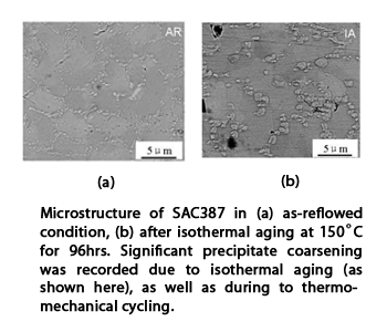
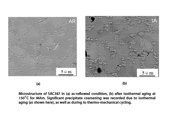
Creep behaviour of lead-free Sn-3.8%Ag-0.7%Cu (SAC387) solder was studied. The ball array grid (BGA) shaped samples were isothermally aged under various temperature-time conditions, and were creep tested at different stresses and temperatures. The effects of aging on the microstructural evolution of the solder was studied and analytically correlated with the creep behaviour of solder joints. A microstructurally adaptive creep model for Sn-based lead-free solder joints was developed which can accommodate the thermo-mechanical history of the solder and predict the primary-cum-secondary creep behaviour of a solder joint.
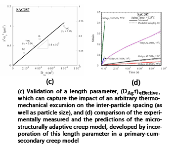
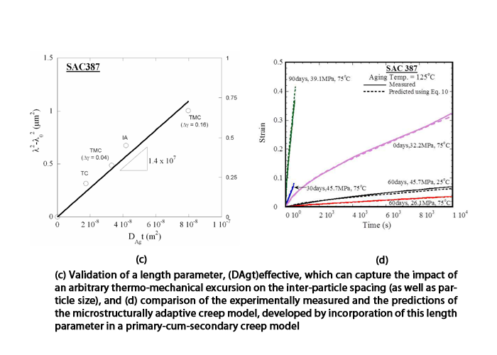
Currently, we are studying the effect of solder composition and electric current on creep of solders (bulk as well as joints). Anwesha Kanjilal is leading this effort.
Relevant References
2. P. Kumar, Z. Huang, I. Dutta, G. Subbarayan and R. Mahajan, book chapter to appear in Lead-free Solders: Materials Reliability for Electronics, edited by K. N. Subramanian, Wiley series in Electronic and Optoelectronic Materials, John Wiley, 2011.
3. Dutta, P. Kumar and G. Subbarayan, J. Metals 61 (06) (2009) 29
4. P. Kumar, O. Cornejo, I. Dutta, G. Subbarayan and V. Gupta, IEEE 10th Proc. EPTC (2008) 903
IMC Growth Kinetics
Currently, the effects of thermo-mechanical excursions on the growth kinetics of intermetallic compounds (IMCs) at the Metal-Sn interface are being studied. We are looking into this problem through two methods: (i) Diffusion couple method. Varun Baheti is working on this problem and we are collaborating with Professor Aloke Paul on this issue, and (ii) Reflow method. Anwesha Kanjilal is leading this effort.
Relevant References2. P. Kumar, B. Talenbanpour, U. Sahaym, C. H. Wen and I. Dutta, IEEE - Proc. ITherm (2012) 880. (Best paper award)
3. P. Kumar, O. Cornejo, I. Dutta, G. Subbarayan and V. Gupta, IEEE - Proc. EPTC (2008) 903
Effects of thermal cycling on integrity of through silicon vias (TSVs)
TSVs are used in advanced, new generation 3-D microelectronic packages to connect electronic circuitries at various levels/layers.
http://en.wikipedia.org/wiki/Through-silicon_via
Thermal cycles with various ΔT ranges, and heating & cooling rates were imposed on Cu filled TSVs in both as-fabricated and annealed conditions. Due to thermal cycling, Cu pillars either intruded or extruded relative to Si jeopardizing integrity of the TSV containing microelectronic package. The extent of intrusion or extrusion of Cu depended on the annealing conditions, heating & cooling rates, and the ΔT range of thermal cycles. An analytical model explaining results was also developed.
We are currently developing FEM based understanding of metal pumping, plasticity, creep and interfacial sliding phenomenon in metal-Si systems. Dipali Sonawane is working on this problem.
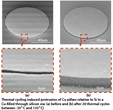

2. I. Dutta, P. Kumar and M. S. Bakir, J. Metals 63(10) (2012) 70
High Strain Rate Fracture of Solder Joints
We are interested in studying fracture behavior of solder joints under mixed mode loading conditions and at high strain rates - mimicking the fall condition. We are currently also performing fracture tests on highly miniaturized solder joints. We are collaborating with Professor Indranath Dutta (Washington State University, Pullman, USA) in this area.
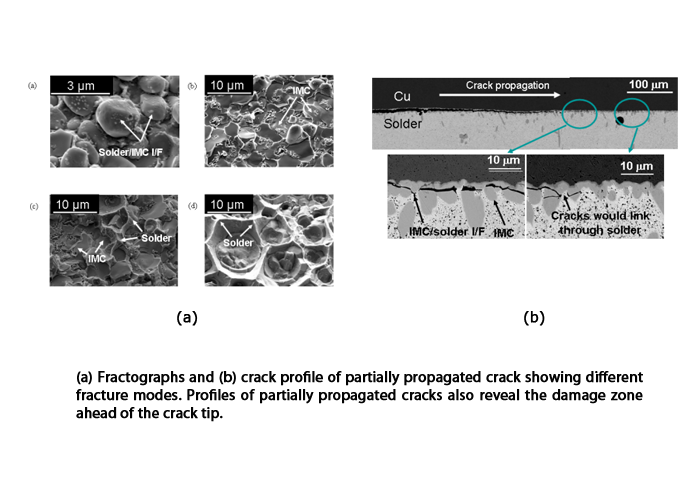
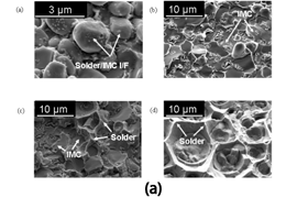
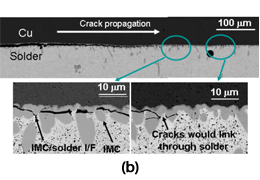
(a) Fractographs and (b) crack profile of partially propagated crack showing different fracture modes. Profiles of partially propagated cracks also reveal the damage zone ahead of the crack tip.
A test fixture was designed to study the mixed-mode fracture behaviour of SAC387 (Sn-3.8%Ag-0.7%Cu)/Cu joints at high strain rates (up to 200 per second ). The effects of strain rate, solder microstructure and the morphology of intermetallic compounds (IMCs) layer at Cu/solder interface were studied, and a fracture mechanism map was developed.

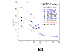
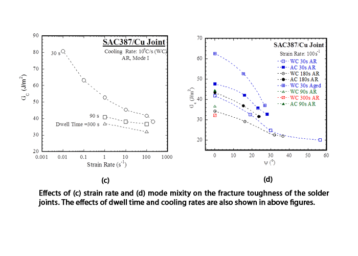
Effects of (c) strain rate and (d) mode mixity on the fracture toughness of the solder joints. The effects of dwell time and cooling rates are also shown in above figures.
A solder microstructure facilitating low yield strength, and a smooth, thin IMC layer yielded high fracture toughness for all testing conditions, although the relative differences in the fracture behaviour (toughness and crack propagation mechanism) diminished at high strain rates as well as at high mode-mixites.
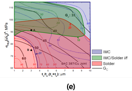
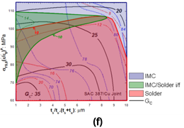
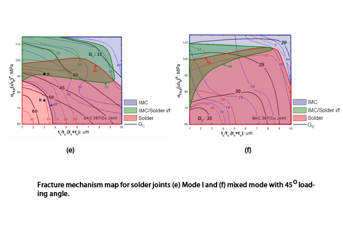
Fracture mechanism map for solder joints (e) Mode I and (f) mixed mode with 45o loading angle.
Relevant References
3. Z, Huang, P. Kumar, I. Dutta, J. H. L. Pang and R. Sidhu, Engineering Fracture Mechanics 131 (2014) 9.
4. Z. Huang, P. Kumar, I. Dutta, R. Sidhu, M. Renavikar and R. Mahajan, J. Elect. Mater. 43 (2014) 88. (Editors' choice for 2013, Freely available)
5. Z. Huang, P. Kumar, I. Dutta, R. Sidhu, M. Renavikar and R. Mahajan, J. Elec. Mater. J. Elec. Mater. 41 (2012) 375
6. P. Kumar, Z. Huang, I. Dutta, R. Sidhu, M. Renavikar and R. Mahajan, J. Elec. Mater. J. Elec. Mater. 41 (2012) 412
7. P. Kumar, Z. Huang, I. Dutta, G. Subbarayan and R. Mahajan, book chapter to appear in Lead-free Solders: Materials Reliability for Electronics, edited by K. N. Subramanian, Wiley series in Electronic and Optoelectronic Materials, John Wiley, 2011.
8. P. Kumar, Z. Huang, I. Dutta, R. Mahajan, M. Renavikar and R. Sidhu, Proc. InterPACK-2009 (ASME) – Vol. 1, San Francisco (USA), July 19 – 23 (2009) p 389
9. P. Kumar, I. Dutta, V. Sarihan, D. R. Frear, S. Jadhav and M. Renavikar , ITherm (IEEE/ASME), (2008) 660
