-
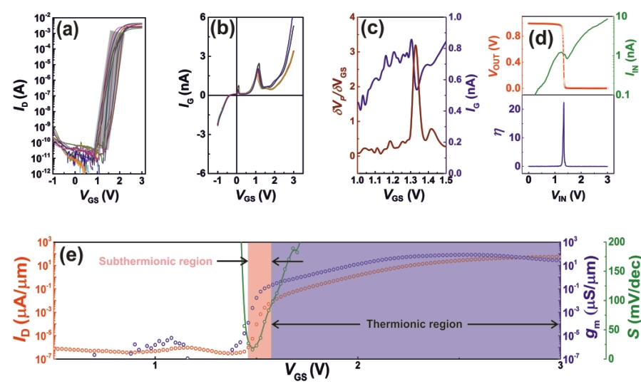
Figure: a) The transfer characteristics of 14 MIMSFET devices (a-IZO annealed at 350 °C) are summarized. b) The gate voltage-gate current plots of four MIMSFETs; the sudden and sharp drop in the gate current represents the negative capacitance behaviour. c) Further verification of the negative capacitance behaviour; the probe voltage (measuring the bulk electrolyte potential) placed in between the gate and the channel shows a sharp rise in ∂VP/∂ѱs reaching a value greater than 3. d) Printed transistor-resistor (≈1 MΩ) inverter with one MIMSFET shows unusually sharp transition and a signal gain of 23. e) A typical transfer characteristic of the printed MIMS FET device, where the a-IZO layer has been annealed at 350 °C, showing the specific drain current and transconductance variation over the entire applied gate voltages; the subthermionic and thermionic transport regimes are marked, the subthreshold slope shows a minimum at around 1.5 V, VGS, where the value dips to 16 mVdec−1. (Adopted from Wiley Behera et. al, Adv. Elect. Mater (2019))
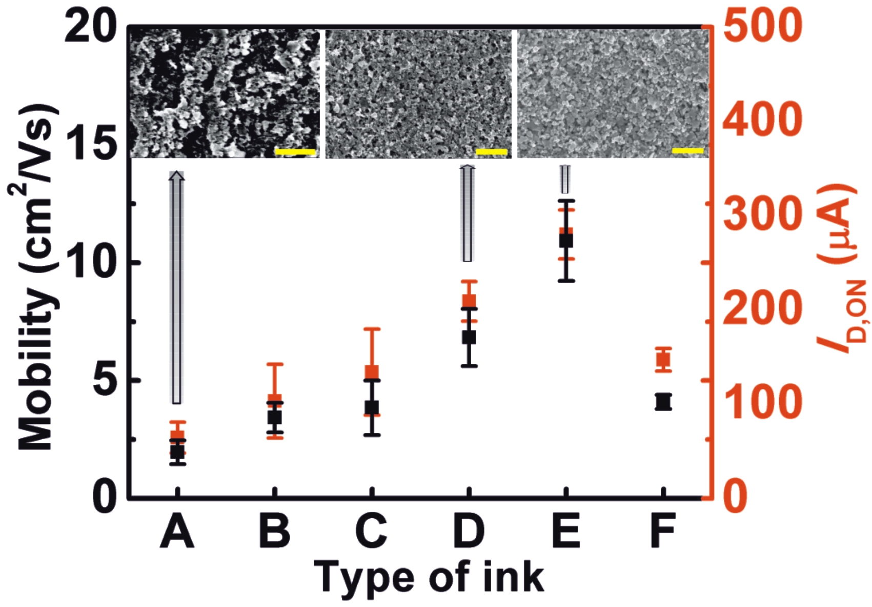
A novel approach has also been developed to lower the process temperature of printed oxide electronics; here an oxide (In2O3) nanoparticulate ink is stabilized using low temperature sublimating aromatic surfactants (e.g. thymol), which sublimates near room temperatures (40 °C), however, in to ensure a complete removal of the organic residue, the printed films have underwent a short heating step at 100 °C, which is nonetheless a temperature that can be suitable to one of the most inexpensive polymer substrate materials, such as polyethylene terapthalate (PET). The surface homogeneity of the nanoparticulate films has been proven to be directly related to the electrical performance obtained; a maximum filed-effect mobility of 13.5 cm2/Vs alongside an on/off ratio >107 have been demonstrated at a processing temperature, as low as 100 °C.
Field-effect mobility as a function of printed semiconductor film morphology; (Adopted from Wiley Divya et. al, Adv. Elect. Mater (2019))
Printed Electronics from inorganic Semiconductors
Besides the organic semiconductors, oxides are the most studied semiconductor material for printed electronics; a large variety of oxide semiconductors has been solution-processed or printed using various jetting or replication-type printing techniques. The major challenges in printed oxide electronics are high process temperatures, limited printing resolution, high variability, low device lifetime, limited mechanical reliability, and absence of reports that demonstrate complete printability including the passive elements. In our laboratory we are addressing all these above mentioned issues individually.
In2O3 Nanoparticles based high performance TFTs on PET substrate
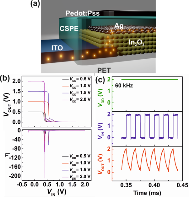
A protocol to fabricate high performance thin film transistors (TFTs) and inverters based In2O3 nanoparticles with process temperature <100 °C and on PET substrate has been developed. The printed depletion-load inverters have shown high signal gain >200 and high frequency operation up to 300 kHz. The high perfromance steps from the deep subthreshold operation and an edge-FET device architecture that allows near vertical transport and shortening of the channel lengths to the thickness of the printed semiconductor layer. The device geometry and the near-vertical transport also make such oxide TFTs and logic units extremely strain tolerate to the tune of 5% tensile strain, during bending fatigue tests down to a bending diameter of 1.5 mm.
Figure: (a) Schematic representation of the In2O3 nanoparticle channel edge-FET device. (b) Voltage transfer characteristics and gain (η) values of the depletion-load type inverter at different supply voltages. (c) The dynamic response of In2O3 nanoparticle based depletion-load inverter at a supply voltage of VDD= 2 V and operating at a frequency of 60 kHz. (Adopted from Wiley Divya et. al, Small(2022))
Inkjet printed large area co-continuous mesoporous structure for device application
Methods have also been developed to print high surface to volume ratio co-continuous mesoporous structures of a large variety of binary and multi-component/ doped oxides with diverse electronic properties (metallic/ semiconducting/ insulating). The process involves use of easy to procure, inexpensive and non-toxic precursors; highly scalable, large-area and high-throughput printing of the mesoporous materials have been demonstrated. The high surface-to-volume ratio of these materials can be exploited in 3D/ bulk field-effect devices, or large production of high performance devices, where surface adsorption or surface chemistry is of importance, such as microsupercapacitors, sensors etc.
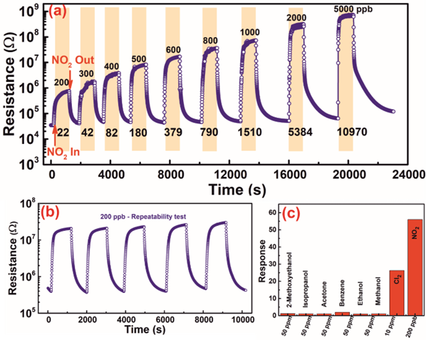
The inkjet printed large area co-continuous mesoporous structure have also been exploited to obtain fully printed gas sensors with ultra-low detection limit and good linearity for NO2 detection, extremely high average response of 11507 at 5 ppm of NO2 along with a short response and recovery time at low operating temperature of 175 °C have been achieved. On the other hand, the sensors when tested for ultra-low detection limit, down to 20 ppb, has shown an easy to amplify response of 31. The stability and selectivity of the fabricated sensor has also been demonstrated.
Figure (a) Printed mesoporous SnO2 sensor response with respect to NO2 gas concentration from 200 ppb – 5000 ppb. (b) Repeatability of the printed 1-layer SnO2 sensor performance to 200 ppb, measured at 175 °C. (c) Selectivity test of the fabricated gas sensor; comparison with common reducing volatile organic compounds (VOCs), such as 2-methoxyethanol, isopropanol, acetone, benzene, ethanol and methanol and an oxidizing gas chlorine measured at 175 °C, with 50 ppm of VOC concentration in each case. (Adopted from ACS Devabharthi et. al, Acs. App. Mat.Interfaces (2021))
Printed two-dimensional transistors and circuits
Two dimensional semiconducting films have poor performance because of their inter-flake transport which limits their conductivity. Here,
fully printed electrolyte-gated MoS2 edge-FETs with predominantly intra-flake carrier transport has been demonstrated. Exploiting the novel device architecture,
printed narrow-channel FETs have been realized, where an additional metal layer is printed onto the 2D-TMD channel and thereby substantially shortens the channel lengths.
Consequently, the printed MoS2 FETs show simultaneous high current saturation and On-Off ratio, with maximum drive currents >310 µA/µm, On-Off ratio >107.
In addition, a channel capacitance modulation induced subthermionic transport, resulting in minimum subthreshold slope ~7.5 mV/dec, has been recorded.
A depletion mode inverter has been demonstrated with a maximum gain of 16. Also, universal logic gates have been demonstrated with a maximum operating frequency
of 10 kHz. The proposed device architecture can be a universal geometry to resolve the network resistance issues in printed 2D electronics.
(Adopted from Wiley S. Mondal et. al. Small Methods (2022) )
Subthermionic transport using tunable electrolytic capacitance distribution in printed electrolyte gated TFTs
Adopting a novel metal-insulator-metal-semiconductor (MIMS) architecture, we have able to fabricate narrow channel field-effect transistors (FETs) with On-current and transconductance values exceeding 200 μAμm−1 and 200 μSμm−1, respectively, however, without compromising on their high On/Off ratio≈ 109. At the same time the new device concept has ensured a body factor (m = ∂VGS/∂ѱs ) of less than 1, which leads to a subthreshold slope lower than the Boltzmann limit (60 mVdec−1 at 300 K). In fact, we observed a subthermionic transport for over four orders of magnitude with values as low as 16 mVdec −1.
Sublimating stabiliser derived low temperature processing of printed inorganic oxide TFTs
Printed micro-supercapacitor arrays
Symmetric as well as asymmetric microsupercapacitors are printed using commercial inkjet printers. Various systems that demonstrate either electric charge double layer (EDLC) or large degree of pseudocapacitor behavior have been studied for extremely large gravimetric and areal capacitance, large cyclic stability etc.
Printed multi-sensor platform
Fully printed gas/ chemical/ humidity/ UV-visible light/ temperature/ pressure sensors are being fabricated and integrated onto an identical substrate/ platform to be addressed in tandem using wireless communication (e.g. NFC) protocols.