
I am currently Assistant Professor in the Department of Materials Engineering, Indian Institute of Science (IISc), Bangalore, India. During my last ten years research journey, I worked with more than 10 different nationality researchers and faculties. I experienced, one of the major benefits of working in a multicultural society is that the cultural exchange of ideas, values, and habits, which helped me a lot in increase my quality of life and depth understating of my research area. Clean and renewable energy is perhaps one of the most important research areas at the current moment for our green and sustainable future. My work is interdisciplinary in nature involving physics, chemistry, materials science, metallurgical engineering, and more. This diverse expertise helps us to deal with a wide range of issues across the fields of nanotechnology and advanced functional materials for energy harvesting, storage, and conservation. I am strong believer that fundamental science very important for next generation technology development. My vision is extending current knowledge in solar cell field using detail and depth fundamental investigation of semiconductors. My primary research interests and experience are in the understanding and improving, emerging material-based device performance. Our research is focused on the optical and electronic properties of novel nanoscale semiconductor systems for a wide variety of energy applications.
- Group Leader and Assistant Professor
- Faculty In-Charge of Strategic Industry Relations, Advanced Facility for Microscopy and Microanalysis (AFMM)
- Faculty In-Charge of Placements, Department of Materials Engineering, Indian Institute of Science (IISc)
Publications in Referred Journals
Research papers: 140+
h-index: 33
i10-index: 86
Citations: 3245
Patent: 3
Book Chapter: 1
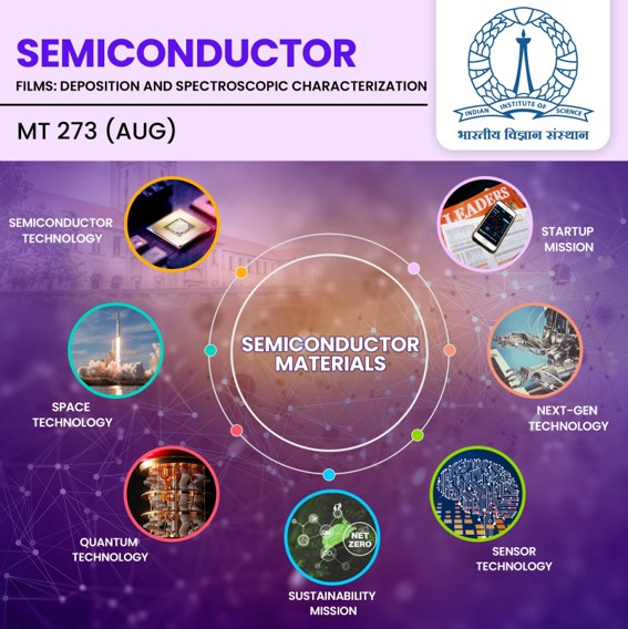
MT 273 (AUG) 3:0
Semiconductor Films: Deposition and Spectroscopic Characterization
Instructor: Sachin R. Rondiya
This course focuses on the imparting fundamental understanding of the working principles of advanced high vacuum deposition techniques used for the fabrication of semiconductor thin films and devices. The necessary theoretical background, important mechanisms associated with growth of films, and the working principles of various optical spectroscopic techniques will be covered.
Semiconductor fundamentals: Common semiconducting materials and their crystal structures; Intrinsic and extrinsic point defects in semiconductors; Electronic band structure; Defect states and their influence on semiconducting properties.
Thin film growth processes: Nucleation and growth mechanisms; uncorrelated or random deposition; surface diffusion-controlled growth; ballistic deposition; shadowing effects, etc.
Thin film deposition techniques: Hot-wire chemical vapor deposition (HW-CVD); plasma-enhanced chemical vapor deposition (PE-CVD); atomic layer deposition (ALD); pulse laser deposition (PLD); RF sputtering, physical vapor deposition (PVD); DC sputtering; Molecular Beam Epitaxy (MBE); thermal evaporation; etc.
Spectroscopic characterization of semiconductors: Ultraviolet-visible-near infrared spectroscopy (UV-Vis-NIR); photoluminescence spectroscopy (PL); time-resolved photoluminescence spectroscopy (TRPL); transient spectroscopy (TAS); etc.
Hands-on laboratory sessions: Hands-on laboratory sessions and practical demonstrations will be conducted for a few high vacuum deposition techniques and spectroscopic measurements for a few semiconductors’ thin films.
References
Thin Film Deposition: Principles and Practice by Donald L. Smith
Spectroscopic Methods in Organic Chemistry by Dudley H. Williams and Ian Fleming
Principles of Instrumental Analysis by Douglas A. Skoog, F. James Holler, and Stanley R. Crouch
Introduction to Spectroscopy by Donald L. Pavia, Gary M. Lampman, George S. Kriz, and James R. Vyvyan
Handbook of Deposition Technologies for Films and Coatings by Peter M. Martin
Handbook of Compound Semiconductors: Growth, Processing, Characterization, and Devices” edited by Paul H. Holloway and Craig T. Lin
Handbook of Deposition Technologies for Films and Coatings by Peter M. Martin
Photoluminescence Spectroscopy of Semiconductors by D. Bimberg, M. Grundmann, and N. N. Ledentsov
Handbook of Optical Constants of Solids by Edward D. Palik
Handbook of Solid-State Lasers: Materials, Systems, and Applications edited by B. Denker and K. Mehrl
Course Title: Solar PV Manufacturing and Packaging
Instructor: Sachin R. Rondiya and Praveen Ramamurthy
This course covers manufacturing and packaging strategies for Silicon, Perovskite, and Thin-Film PV modules, preparing students for careers in PV R&D and industrial production.
Module 1: Industrial Solar Cells ” From Lab to Fab
Covers key differences between lab-scale and commercial PV manufacturing. Topics include Crystalline Silicon processes (ingot growth, wafering, doping, module assembly), Thin-Film techniques (CVD, sputtering, encapsulation), and scalable Perovskite/Tandem PV processes addressing stability and integration.
Module 2: Deposition, Solution Processing & Doping Techniques
Deposition: CVD, sputtering, co-evaporation, inkjet printing (thin-film); spin, blade, slot-die, vapour deposition (perovskites).
Large-Area Processing: Scalable coating methods (slot-die, inkjet) for perovskite/tandem modules; film uniformity and defect control.
Doping & Ancillary: Boron/phosphorus diffusion (Si), alkali treatments (CIGS), perovskite tuning, metallisation, encapsulation, and reliability testing.
Module 3: Packaging & Moisture Control
Explores PV module structure (cells, encapsulants, back/front sheets, junction boxes), mechanical/optical/electrical/moisture protection, and key failure modes. Covers encapsulant properties (EVA, POE, TPU), degradation, gel content, WVTR requirements, test methods (Ca-test, MOCON, CRDS), sealing challenges, and durability comparisons of glass vs. polymer sheets.
Module 4: Manufacturing Integration & Reliability
Lamination parameters (temperature, vacuum, pressure, dwell), inline QC (peel, gel, thermal), edge sealing, and junction box integration for various module types (glass-glass, bifacial, flexible). Discusses defect detection (EL, IR, IV), packaging failures (delamination, yellowing, corrosion), environmental stress testing (UV, heat, humidity), and standards (IEC 61215/61730, UL 1703).
Hands-on laboratory: (1) WVTR measurements (Calcium Degradation, CRDS); (2) Degradation analysis under damp heat and UV; (3) PV module teardown for packaging layer analysis; (4) Utilise EL and IR imaging to detect packaging-related defects.
References:
Solar Cells: Materials, Manufacture and Operation: Edited by Tom Markvart and Luis Castner: Publisher Elsevier
Advanced Characterisation Techniques for Thin Film Solar Cells: Edited by Daniel Abou-Ras, Thomas Kirchartz, Uwe Rau
Physics of Solar Cells: from Principles to New Concepts by Peter Wurfel: Publisher Wiley-VCH Verlag GmbH & Co. KgaA
Fundamentals of Solar Cells: Photovoltaic Solar Energy Conversion by Alan L Fahrenbruch and Richard H Bube: Academic Press
Cu(In1-xGax)Se2 Based Thin Film Solar Cells: Edited by Vladimir Agranovich, Volume 35, Publisher Elsevier.
Copper Zinc Tin Sulfide-Based Thin-Film Solar Cells: Edited by KEntaro Ito. Publisher Wiley.
Vacuum Technology: Edited by Alexander Roth. Publisher Elsevier.
Chemical solution deposition of semiconductor films: Edited by Gary Hodes. Publisher Marcel Dekker, Inc.
Organic Inorganic Halide Perovskite Photovoltaics From Fundamentals to Device Architectures: Edited by Nam-Gyu Park Michael Grätzel Tsutomu Miyasaka. Publisher Springer.
Photovoltaic Materials: Edited by Richard H, Bube. Publisher Imperial College London Press.
2022
Nanotechnology (IOP) Journal. Topic: Focus Collection Perovskite-Inspired Materials (I.F. – 3.8)
Details: https://iopscience.iop.org/journal/0957-4484/page/perovskite-inspired-materials-energy-applications
2022
Frontiers in Materials Journal. Topic: Chalcogenide Compounds for Energy (I.F. – 3.5)
Details: https://www.frontiersin.org/research-topics/32056/emerging-chalcogenide-compounds-for-energy-conversion-and-storage-applications
Professional Recognitions
2024
Elected as a “Fellow” of Maharashtra Science Academy, India.
2022
Elected as a “Young Scientist Award” at International Conference on Material Manufacturing, USA.
2021
Elected as a “Foreign Young Associate” of the Maharashtra Academy of Sciences, India.
2020
Member of Editorial Board of International Journal of Materials Science and Applications.
2020
Member of Editorial Board of Materials Journal (MDPI).
Scientific Reviewing Activities
Currently a reviewer for the following scientific journals: Nature: Scientific Report, Journal of Alloys and Compounds, Journal of Physics and Chemistry of Solids, Materials Today: Proceedings, ACS Applied Electronic Materials, Coatings, Solar Energy Materials and Solar Cells, Vacuum, Crystals, AIP Advances, ACS Applied Electronic Materials, etc.
Outreach Activities
(1) Education Activities: Education is the key to empowering young people to improve their lives and contribute to society. A quality education is the top priority that every institute strives to maintain, as it plays a vital role in India’s progress. Over the past ten years, I have actively been involved in many outreach activities, both independently and through various organizations. My focus has been on the following three categories, which help youngsters, students, and faculty members gain valuable information, confidence, and skills necessary for quality education, research, and a better life.
(2) Prevent Suicide in Youth/Students ” Since 2014, I have been closely working with various groups and actively supporting a few important missions focused on Indian youth, particularly in the area of suicide prevention, which is a major concern. I have engaged in student counseling, open discussions, and initiatives to provide a platform where students can ask questions and seek guidance. I have delivered more than 20 talks, seminars, and webinars on various platforms, focusing on building resilience and developing a strong, warrior-like attitude among young students. Additionally, I have been consistently working to support suicide prevention efforts for the well-being of youth.
(3) Mentoring and Academic Development Initiatives: Over the past decade, I have actively contributed to academic mentoring and faculty development through two major initiatives. Firstly, in the area of Career Opportunities in Research and Industry, I have delivered more than 25 invited talks at various colleges and institutes, mentoring master’s students on diverse career paths in research and industry. With over 10 years of research experience, I strive to share valuable insights with both students and faculty members, helping them make informed career decisions. Secondly, through Faculty Development Programs, I have been working closely with teachers and faculty members from small villages and cities since 2012, organizing one-day workshops aimed at enhancing teaching methods and research awareness. As part of this initiative, I have visited numerous schools and colleges across India. These programs were thoughtfully designed to bridge the gap in research exposure and modern teaching skills necessary for contemporary higher education in the country.